Circuit Schematic Design
Whenever you are designing products, especially electronic ones, the end goal is often to have a Printed Circuit Board created.
You need a design for schematic circuit as the first step to making a Printed Circuit Board.
The designing process for the schematic circuit requires that you do your research early enough, which was mentioned in the preliminary stages above.
You may however, also need to run some simulations together with broad-boarding, especially if your product is a modern electronic.
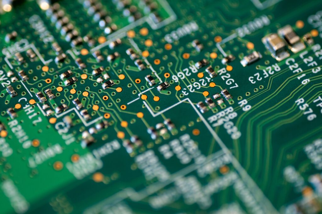
Designing the Printed Circuit Board
The layout for the Printed Circuit Board is created using the same software package as the one used in the circuit schematic design.
Part of it may be routed automatically, although a better part of it has to be routed using a manual system for the product’s performance to be very optimum.
The printed circuit system is extremely sensitive for radio frequency circuits such as WIFI, GPS and Bluetooth; and also, for power. Because of this, it is very easy to make mistakes in these areas. Great caution must be taken for this reason.
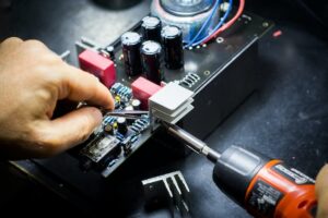
Debugging and Evaluation of the Prototype
Once you get the Prototype back, you then need to find out whether or not there are any problems in it and debag appropriately.
Debagging of a new circuit in an electronic product that is being developed is quite a difficult procedure.
This is because you can only know how long it takes to get the problem fixed, once you have established what exactly the problem is.
Microcontroller Programming
All electronic products have some sort of microcontroller that act as the main point of functionality and brains for the product.
All the microcontrollers are often computer programmed with a special language to ensure that they are operating well.
Some of the program’s parts need to be done in an assembly language to ensure that they are operating properly and efficiently.
Design of the Enclosure System

This is often mostly done by a different Engineer, from the one that handles the different procedures discussed above.
So long as you have a good idea of what you want your product to look like, then you may decide to have an expert who is familiar with 3D modeling to this do for you.
Thereafter, you may have to look for the services of an engineer who deals with industrial design for your product to look appealing.
The specialist you choose to hire to help with the 3D design modelling has to be someone who is well experienced with the technology of molding.
Of importance to note is the fact that low volume prototyping uses 3D printing; whereas manufacturing of high-volume capacity can make use of injection molding.
Circuit Boards for VoIP
A VoIP SIP PCB solution is designed with the person in mind. The VoIP SIP Circuit telephone board gives new opportunities in tasks wherein you combine your VoIP communication system solution. It offers a smooth to function and crystal sound quality. As a relied-on provider for emergency cellphone systems, it is great in feature and performance. VoIP circuit boards need to come with a variety of features such as; call holding, call forwarding, call holding, hot lines, DND, mute, speed dial and more. You need to choose a board with all the features you will need. Looking at VoIP phones reviews will give you all the information you need to choose the right provider for your business needs.
Conclusion
The whole idea of creating a new product can be very thrilling. However, there is so much that needs to be considered in the process of developing a product. The various steps and considerations that needs to be taken will help you design your product in readiness for manufacture. When you narrow down your concept about a product, then you are able to transform it from a notion that is ambiguous and broad, into a specific product that you can easily work on.